Table of Contents
Analog Input
The analog inputs of the ZSOM-Control and the ZSOM-Mini are grouped by ADC chips with 6 channels each. All channels of a group are sampled simultaneously and share the same input range.
Features
| ZSOM-Control | ZSOM-Mini | |
|---|---|---|
| Number of channels | 12 (2 groups × 6) | 6 (1 group) |
| Groups | ADC1: AIN1–AIN6, ADC2: AIN7–AIN12 | ADC1: AIN1–AIN6 |
| Resolution | 16 bit | 16 bit |
| Range | ±5 V or ±10 V, selectable per group | ±5 V or ±10 V |
| Sampling rate | up to 450 kHz, selectable per group | up to 450 kHz |
| Sample and hold | simultaneous per group | simultaneous |
| Anti aliasing | 4th order, fg = 200 kHz | 4th order, fg = 200 kHz |
| Maximum input voltage | ±32 V | ±32 V |
| Power | always on | requires GPIOs ENVP and ENANALOG, see Power and GPIOs |
| Terminals | AIN1–AIN12 on pins 23–45 (odd), AGND in between (pinout) | AIN1–AIN6 on pins 45–55 (odd), AGND in between (pinout) |
Use AGND (not GND) as reference for the analog signals.
Connecting a signal
The signal is routed through the following stages after the screw terminal:
- Impedance converter
- Anti aliasing filter
- Analog to digital converter
Impedance converter
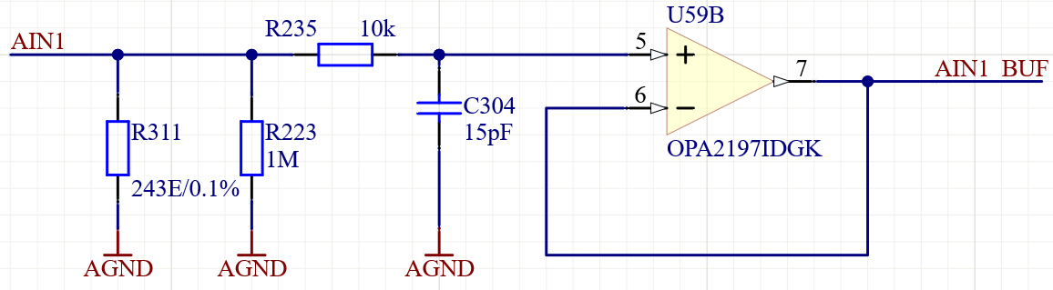
current hardware version ZSOM-Control V1.2 and newer ZSOM-MINI V1.1 and newer
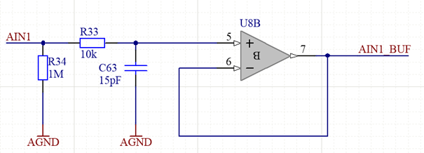
hardware versions ZSOM-Control V0 .. V1.1
This schematic shows the first stage of the input circuit of one Analog Input channel.
The input is optimized for low or mid impedance voltage signal sources.
The 243 Ω shunt (R311) is not fitted by default. It can be used to transform the inputs to sense current signals such as 4–20 mA standard signals.
To adapt for high impedance signal sources, current sources or other special signal sources, please contact Schmid Elektronik for advice.
Anti aliasing filter
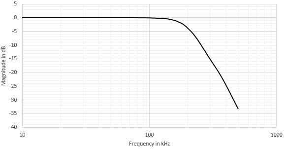
This graph shows the frequency response of the 4th order anti aliasing filter. This characteristic has to be considered if the measured signal consists of frequencies above 100kHz.
Analog to digital conversion
The ADC chips have sample and hold functionality. This means, that all signals in a group of 6 channels per chip are sampled simultaneously at exactly the same time.
Usage in LabVIEW
The ADCs are read in the FPGA with the ADC FPGA driver VIs of the SDK. The input range is set per group with these VIs:
- ZSOM-Control: CLIP items ADC1_RANGE / ADC2_RANGE, TRUE = ±5 V, FALSE = ±10 V
- ZSOM-Mini: GPIO ADC RANGE (see Power and GPIOs), TRUE = ±5 V, FALSE = ±10 V
Examples in the SDK:
- ZSOM-Control: ZSOM-Control_ADC_burst.lvproj
- ZSOM-Mini: ADC burst example and ZSOM-Mini-ALLIO.lvproj