Table of Contents
ZSOM-Control Pinout description
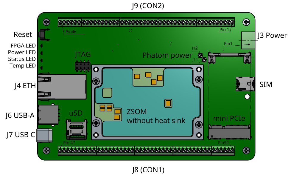
The process I/O signals of the ZSOM-Control are available on two screw terminal blocks. The pin numbers are printed on the PCB next to the terminals:
- J8 (CON 1): pins 1–46 – digital inputs, analog outputs and analog inputs
- J9 (CON 2): pins 47–92 – switchable supply outputs, CAN, RS422/RS485, RS232, DIO and open collector outputs
With the PCB labelling readable (upright), J9 is the upper row with pin 47 at the top left, and J8 is the lower row with pin 1 at the bottom right. The table follows the connectors from left to right and shows opposite pins side by side (pin 47 is opposite pin 46, pin 92 opposite pin 1).
Screw terminals
| J9 Pin | Signal | . | J8 Pin | Signal |
|---|---|---|---|---|
| 47 | +5V (switchable) | 46 | AGND | |
| 48 | GND | 45 | AIN12 | |
| 49 | +3.3V (switchable) | 44 | AGND | |
| 50 | GND | 43 | AIN11 | |
| 51 | CAN High | 42 | AGND | |
| 52 | CAN Low | 41 | AIN10 | |
| 53 | GND | 40 | AGND | |
| 54 | RS422/RS485 TX+ | 39 | AIN9 | |
| 55 | RS422/RS485 TX- | 38 | AGND | |
| 56 | RS422/RS485 RX- | 37 | AIN8 | |
| 57 | RS422/RS485 RX+ | 36 | AGND | |
| 58 | GND | 35 | AIN7 | |
| 59 | RS232 RTS | 34 | AGND | |
| 60 | RS232 CTS | 33 | AIN6 | |
| 61 | RS232 RX | 32 | AGND | |
| 62 | RS232 TX | 31 | AIN5 | |
| 63 | GND | 30 | AGND | |
| 64 | DIO1 | 29 | AIN4 | |
| 65 | DIO2 | 28 | AGND | |
| 66 | DIO3 | 27 | AIN3 | |
| 67 | DIO4 | 26 | AGND | |
| 68 | GND | 25 | AIN2 | |
| 69 | DIO5 | 24 | AGND | |
| 70 | DIO6 | 23 | AIN1 | |
| 71 | DIO7 | 22 | AGND | |
| 72 | DIO8 | 21 | AOUT4 | |
| 73 | GND | 20 | AGND | |
| 74 | DIO9 | 19 | AOUT3 | |
| 75 | DIO10 | 18 | AGND | |
| 76 | DIO11 | 17 | AOUT2 | |
| 77 | DIO12 | 16 | AGND | |
| 78 | GND | 15 | AOUT1 | |
| 79 | DIO13 | 14 | DIN10 | |
| 80 | DIO14 | 13 | DIN9 | |
| 81 | DIO15 | 12 | GND | |
| 82 | DIO16 | 11 | DIN8 | |
| 83 | GND | 10 | DIN7 | |
| 84 | OC1 | 9 | GND | |
| 85 | OC2 | 8 | DIN6 | |
| 86 | GND | 7 | DIN5 | |
| 87 | OC3 | 6 | GND | |
| 88 | OC4 | 5 | DIN4 | |
| 89 | GND | 4 | DIN3 | |
| 90 | OC5 | 3 | GND | |
| 91 | OC6 | 2 | DIN2 | |
| 92 | GND | 1 | DIN1 |
DIO (general purpose high speed I/O) are labelled GPIO1–16 in the fact sheet.
Power connector (J3)
| Pin | Signal |
|---|---|
| 1 | GND |
| 2 | +VIN, 9–28 V (reverse polarity protected) |
| 3 | Earth |
Other connectors
| Designator | Connector | Function |
|---|---|---|
| J4 | RJ45 | Gigabit Ethernet |
| J6 | USB Type A | USB host |
| J7 | USB Type C | USB device (Ethernet over USB) |
| SD1 | microSD | SD card |
| PCIe1 / SIM1 | miniPCIe slot with nano-SIM holder | 4G modem, GPS receiver or Wi-Fi module |
| J11 / J12 | U.FL | GPS module / GPS antenna, with 5 V phantom supply for active antennas (200 mA PTC fuse) |
| BAT1 | CR2032 holder | Backup battery |
| J10 | 8-pin header | JTAG for the CAN microcontroller – for firmware update and debugging |