Table of Contents
Example: DIO all
This example sets and reads all digital I/O lines on the screw terminals of the ZSOM-Control.
Project: ZSOM-Control_DIO_all.lvproj. In LabVIEW, open Help → Find Examples and search for “ZSOM”.
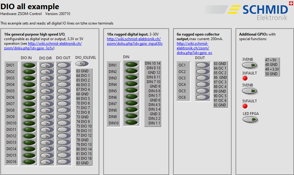
RT code: front panel
Front panel
The front panel is divided into the following groups. The pin numbers of the terminals are printed next to the controls, see also the ZSOM-Control pinout.
| Group | Controls | Indicators | Documentation |
|---|---|---|---|
| 16× general purpose high speed I/O, configurable as input or output | DIO DIR (In / Out), DIO OUT, DIO_IOLEVEL (3.3 V or 5 V) | DIO IN | DIO 3.3 V / 5 V |
| 10× rugged digital input | – | DIN | DIN |
| 6× rugged open collector output | DOUT | – | DOUT (open collector) |
| Additional GPIOs with special functions | 3VENB, 5VENB, LED FPGA | 3VFAULT, 5VFAULT | ZSOM-Control |
How it works
- FPGA (
DIO_all_FPGA_main.vi): Four loops run in parallel: DIN, GPIO, DOUT OC and DIO. They connect the I/O items of the CLIP to the front panel controls and indicators of the FPGA VI. - RT (
DIO_all_RT_main.vi): Loads and starts the FPGA and then writes the controls and reads the indicators in a loop (wait time 50 ms).
Note from the block diagram of the FPGA VI: If a terminal is used only as an input or only as an output, without switching the direction at run time, use zsom.control.fpga.dio_1.init_in.vi or zsom.control.fpga.dio_1.init_out.vi instead of zsom.control.fpga.dio_1.init_io.vi.
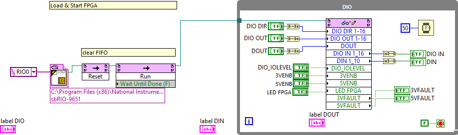
RT code: block diagram
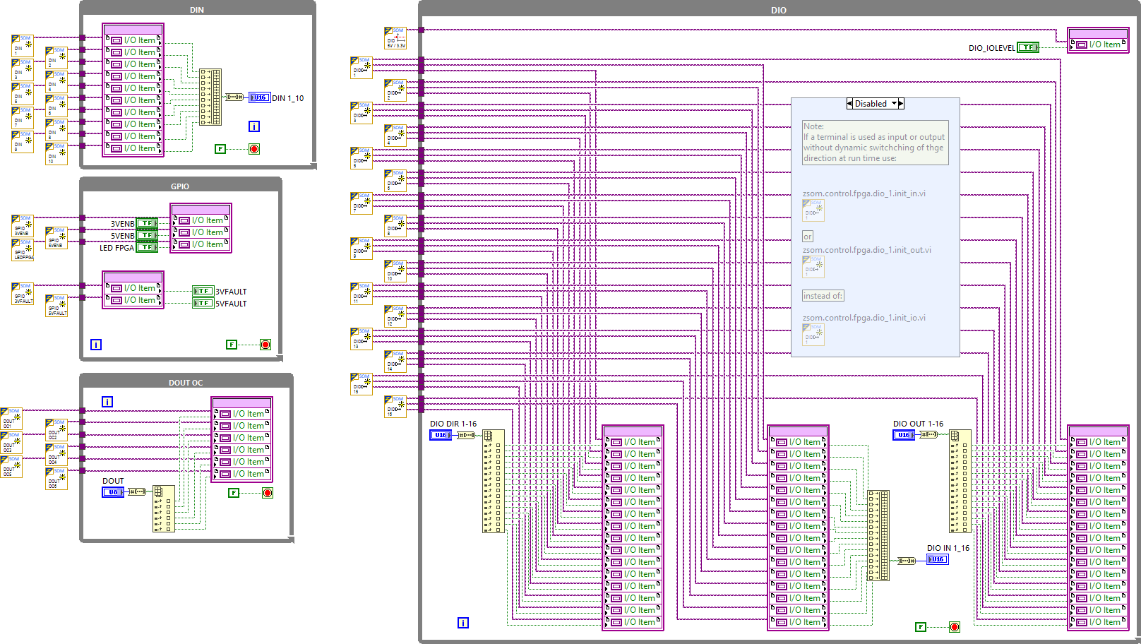
FPGA code: block diagram