Example: Mini GPIO
This example shows how to control the GPIOs that control the power distribution on the ZSOM-Mini. It also reads and writes the digital I/O lines. For the meaning of the GPIOs, see Power and GPIOs.
Project: ZSOM-Mini_GPIO.lvproj. In LabVIEW, open Help → Find Examples and search for “ZSOM”.
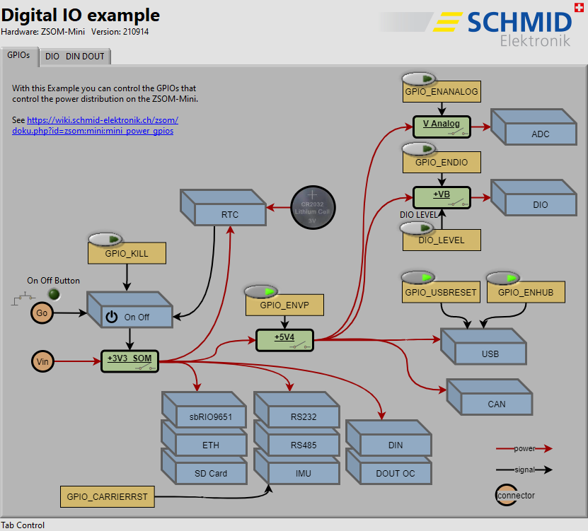
RT code: front panel
Front panel
The front panel has two tabs.
| Tab | Content |
|---|---|
| GPIOs | The power distribution of the ZSOM-Mini as a diagram with the GPIOs that switch the regions: GPIO_ENVP, GPIO_ENANALOG, GPIO_ENDIO, DIO_LEVEL, GPIO_ENHUB, GPIO_USBRESET and GPIO_KILL. The Go input is shown as the On Off button. |
| DIO DIN DOUT | DIO1–DIO10 (direction, output, input), DOUT1–DOUT4 and DIN1–DIN4 |
How it works
- FPGA (
GPIO_FPGA_main.vi): Connects the GPIOs and the I/O lines of the CLIP to the front panel controls and indicators of the FPGA VI. - RT (
GPIO_RT_main.vi): Loads and starts the FPGA. Two loops write the controls and read the indicators: GPIOs (Enable VP, Enable USB, Enable Analog, Enable DIO, DIO LEVEL, RESET\ USB, KILL, On Off Button) and DIO DIN DOUT.
Most regions of the ZSOM-Mini are off by default. To use a region, switch on the corresponding GPIOs first, see ZSOM-Mini Quick start guide.
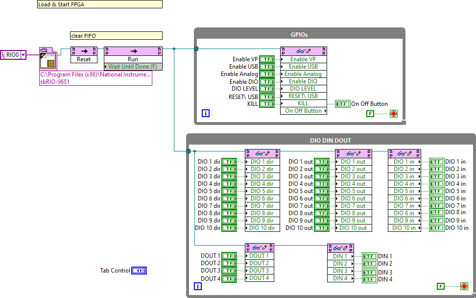
RT code: block diagram
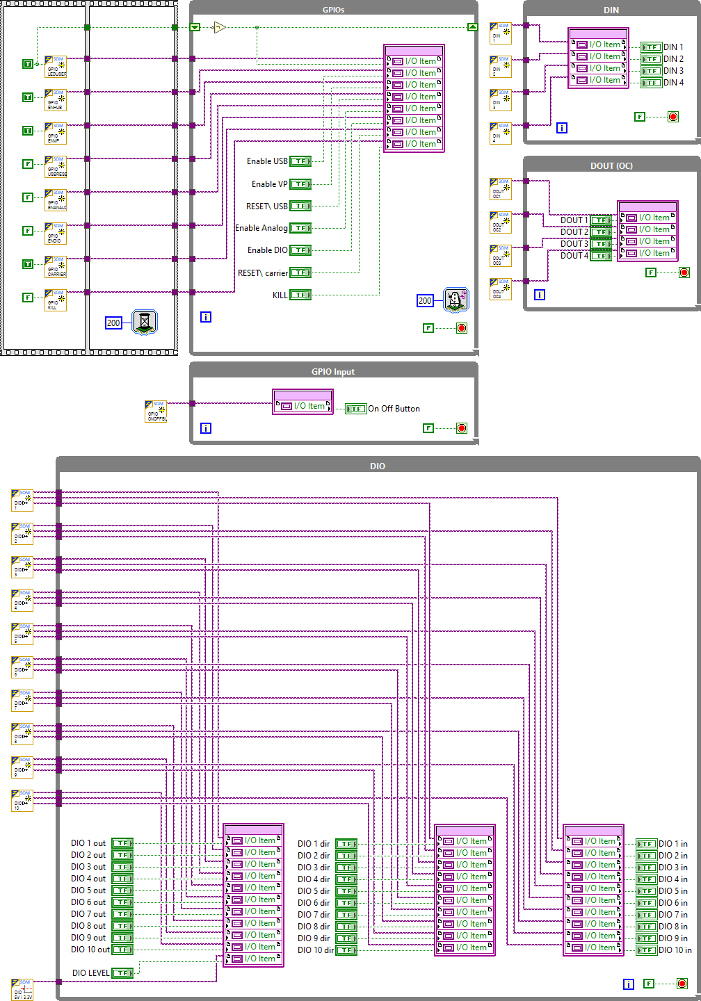
FPGA code: block diagram